|
| Place of Origin: | China |
| Brand Name: | OEM |
| Certification: | ISO9001 |
| Minimum Order Quantity: | Negotiable |
|---|---|
| Price: | Negotiable |
| Packaging Details: | 100 clean bag or single box packaging |
| Delivery Time: | 5-7 working days after received your payment details working days after received your payment details |
| Payment Terms: | T/T, Western Union, L/C |
| CAS: | 25617-97-4 | EINECS No.: | 247-129-0 |
|---|---|---|---|
| MF: | GaN | Appearance: | Crystal |
| Density: | 6.1g/mL,25/4℃ | MW: | 83.73 |
| High Light: | silicon wafer substrate,silicon oxide wafer |
||
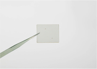
GaN Gallium Nitride Single Crystal Wafer CAS 25617-97-4 with Density of 6.1g/mL
Typical Physical Properties of GaN Gallium Nitride Single Crystal Wafer
2'' GaN Templates
| Item | GaN-T-N | GaN-T-S | |
| Dimensions | Φ 2'' | ||
| Thickness | 15 μm, 20 μm, 30 μm, 40 μm | 30 μm, 90 μm | |
| Orientation | C-axis(0001) ± 1° | ||
| Conduction Type | N-type | Semi-Insulating | |
| Resistivity(300K) | < 0.05 Ω.cm | > 106 Ω.cm | |
| Dislocation Density | Less than 1x108 cm-2 | ||
| Substrate structure | Thick GaN on Sapphire(0001) | ||
| Useable Surface Area | > 90% | ||
| Polishing | Standard: SSP Option: DSP | ||
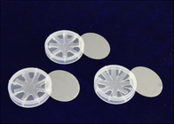
| Package | Packaged in a class 100 clean room environment, in cassettes of 25pcs or single wafer containers, under a nitrogen atmosphere. | ||
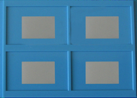
2'' -Standing GaN Substrates
| Item | GaN-FS-N | GaN-FS-SI | |
| Dimensions | Φ50.8mm ± 1mm | ||
| Marco Defect Density | ALevel | 2 cm-2 | |
| B Level | > 2 cm-2 | ||
| Thickness | 350 ± 25 μm | ||
| Orientation | C-axis(0001) ± 0.5° | ||
| Orientation Flat | (1-100) ± 0.5°, 16.0 ± 1.0mm | ||
| Secondary Orientation Flat | (11-20) ± 3°, 8.0 ± 1.0mm | ||
| TTV(Total Thickness Variation) | <15 μm | ||
| BOW | <20 μm | ||
| Conduction Type | N-type | Semi-Insulating | |
| Resistivity(300K) | < 0.5 Ω.cm | >106 Ω.cm | |
| Dislocation Density | Less than 5x106 cm-2 | ||
| Useable Surface Area | > 90% | ||
| Polishing | Front Surface: Ra < 0.2nm. Epi-ready polished Back Surface: Fine ground | ||
| Package | Packaged in a class 100 clean room environment, in single wafer containers, under a nitrogen atmosphere. | ||
![]()
Free-standing GaN Substrates (Customized size)
| Item | GaN-FS-10 | GaN-FS-15 | |
| Dimensions | 10.0mm Χ10.5mm | 14.0mmΧ 15.0mm | |
| Marco Defect Density | ALevel | 0 cm-2 | |
| B Level | 2 cm-2 | ||
| Thickness | Rank 300 | 300 ± 25 μm | |
| Rank 350 | 350 ± 25 μm | ||
| Rank 400 | 400 ± 25 μm | ||
| Orientation | C-axis(0001) ± 0.5° | ||
| TTV(Total Thickness Variation) | <15 μm | ||
| BOW | <20 μm | ||
| Conduction Type | N-type | Semi-Insulating | |
| Resistivity(300K) | < 0.5 Ω.cm | >106 Ω.cm | |
| Dislocation Density | Less than 5x106 cm-2 | ||
| Useable Surface Area | > 90% | ||
| Polishing | Front Surface: Ra < 0.2nm. Epi-ready polished Back Surface: Fine ground | ||
| Package | Packaged in a class 100 clean room environment, in single wafer containers, under a nitrogen atmosphere. | ||
![]()
| Item | GaN-FS-N-1.5 | |||||
| Dimensions | 25.4mm ± 0.5mm | 38.1mm± 0.5mm | 40.0mm ± 0.5mm | 45.0mm ± 0.5mm | ||
| Marco Defect Density | ALevel | 2 cm-2 | ||||
| B Level | > 2 cm-2 | |||||
| Thickness | 350 ± 25 μm | |||||
| Orientation | C-axis(0001) ± 0.5° | |||||
| Orientation Flat | (1-100) ± 0.5° 8 ± 1mm | (1-100) ± 0.5° 12 ± 1mm | (1-100) ± 0.5° 14 ± 1mm | (1-100) ± 0.5° 14 ± 1mm | ||
| Secondary Orientation Flat | (11-20) ± 3° 4 ± 1mm | (11-20) ± 3° 6 ± 1mm | (11-20) ± 3° 7 ± 1mm | (11-20) ± 3° 7 ± 1mm | ||
| TTV(Total Thickness Variation) | <15 μm | |||||
| BOW | <20 μm | |||||
| Conduction Type | N-type | Semi-Insulating | ||||
| Resistivity(300K) | < 0.5 Ω.cm | >106 Ω.cm | ||||
| Dislocation Density | Less than 5x106 cm-2 | |||||
| Useable Surface Area | > 90% | |||||
| Polishing | Front Surface: Ra < 0.2nm. Epi-ready polished Back Surface: Fine ground | |||||
| Package | Packaged in a class 100 clean room environment, in single wafer containers, under a nitrogen atmosphere. | |||||
![]()
HR‐XRD Rocking Curves
![]()
Contact Person: Ms. Linda
Tel: +86-19945681435
Address: Rm 1712-1715, No.88, Sibao Rd, Shanghai , China